Metalens technology is revolutionizing the world of optics by offering a compact and efficient alternative to traditional lenses. Developed from innovative mini-lens concepts, this cutting-edge technology employs metasurfaces to bend and control light with unparalleled precision. Pioneered by Rob Devlin and his team at Metalenz, a startup that emerged from the prestigious Harvard lab of Federico Capasso, the implementation of metalenses is now transforming consumer electronics, enhancing everything from smartphones to high-end tablets. With around 100 million units produced, these light-focusing devices not only reduce costs but also pave the way for new functionalities in devices like the latest iPad and Google Pixel 8 Pro. As demand for advanced optical solutions increases, the impact of Polar ID technology—a groundbreaking application of metalens innovation—signals a new era in how we perceive and interact with our gadgets.
The emergence of lens-making technologies based on metasurfaces marks a significant shift in the optical design landscape. These advanced mini optics offer a streamlined and cost-effective solution for integrating lens functionalities into various electronic devices. Rob Devlin’s startup, Metalenz, is at the forefront of this innovation, focusing on leveraging engineered surfaces to manipulate light in dynamic ways. The integration of Polar ID technology further exemplifies the potential of these meta-optical systems, providing enhanced security features for consumer electronics. As companies race to adopt such transformative technologies, the landscape of optics stands poised for disruption with profound implications across multiple industries.
The Evolution of Metalens Technology
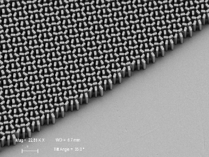
Metalens technology has revolutionized the field of optics by offering compact, efficient solutions for capturing and focusing light. Historically, lenses were crafted from curved glass or polished plastic, making them bulky and expensive. However, the emergence of mini-lens designs, developed through meticulous research at the Harvard lab, represents a significant leap forward. These mini-lenses utilize a series of tiny pillars arranged on a flat surface, allowing for mass production and cost-effectiveness. The collaboration of innovative minds led by Rob Devlin and Federico Capasso is a testament to how academia can fuel industry growth.
The transition from research prototypes to practical applications has been remarkably swift. Within just a few years, metalens technology evolved from initial concepts into fully realized products that are now embedded in mainstream consumer electronics. This rapid development showcases the potential for university-backed startups to disrupt traditional industries, fundamentally changing how devices operate. The success of Metalenz demonstrates a successful fusion of scientific inquiry and entrepreneurial spirit, promising a future where high-quality optics are accessible to all.
The Impact of Metasurfaces in Consumer Electronics
Metasurfaces have become a cornerstone of modern consumer electronics, enhancing functionalities while minimizing space requirements. Devices like smartphones and tablets have greatly benefited from the integration of these innovative light-focusing metasurfaces, allowing manufacturers to incorporate advanced features without the constraints of traditional lens systems. Reports indicate that major brands like Apple and Google are already utilizing these technologies, paving the way for a new era in device design. The ability to create slimmer, more versatile gadgets that maintain high performance is a game-changer in the competitive tech market.
Rob Devlin highlighted the significant role metasurfaces play in advancing practical applications such as facial recognition and augmented reality. By utilizing light in more sophisticated ways, these surfaces can produce precise depth information, leading to improved functionalities in various devices. The collaboration with STMicroelectronics to integrate metasurfaces into 3D sensing modules illustrates how metalens technology is becoming indispensable in creating smarter, more capable devices that cater to evolving user needs.
Harnessing Polar ID Technology for Enhanced Security
The advent of Polar ID technology marks an exciting development in the realm of optical security measures. Utilizing the polarization of light, this innovation offers a new dimension of identity verification. By requiring the unique characteristics of a person’s light reflection, Polar ID presents a cost-effective alternative to traditional polarization cameras that are both bulky and expensive. Rob Devlin’s vision of integrating this technology into everyday devices could significantly enhance security features without compromising on convenience or affordability.
The potential applications for Polar ID extend beyond smartphones. For example, its unique light signature capabilities could benefit the healthcare industry by allowing for more precise detection of skin abnormalities. This aspect of Polar ID highlights the versatility of metalens technologies—bridging consumer electronics and critical medical applications. By leveraging the compact design and low production costs associated with metasurfaces, Polar ID could facilitate the widespread adoption of more secure and health-focused technology in daily life.
The Future of Mini-Lens Technology
As the demand for mini-lens technology continues to surge, Metalenz is committed to pushing the boundaries of innovation. The company’s ability to scale production efficiently is not only a testament to their technological prowess but also an indication of the growing market for sophisticated optical solutions. With a team dedicated to refining existing products while pursuing new developments, the future looks promising for mini-lenses as they pave the way for an array of applications that could redefine consumer electronics.
Rob Devlin’s ongoing collaboration with the Capasso lab suggests that more breakthroughs are on the horizon. Each advancement in mini-lens capabilities brings with it the potential for entirely new product categories, transforming the landscape of consumer electronics. As the global tech industry continues to embrace these advanced optics, we can anticipate a wave of innovations that blur the line between hardware functionality and everyday convenience.
Partnerships Driving Success in Optical Innovation
The journey of Metalenz exemplifies how strategic partnerships can propel technological advancements. By forging collaborations with Harvard’s Office of Technology Development and other institutions, Metalenz has tapped into a reservoir of interdisciplinary expertise. This approach not only enriches product development but also drives a culture of innovation that underpins their success. Partnerships in academia provide startups like Metalenz with unique insights and access to cutting-edge research, making it possible to pioneer captivating optical solutions.
These collaborations are not simply beneficial; they are essential in a fast-paced tech world where staying ahead of competitors is crucial. By working closely with thought leaders and researchers, Metalenz can continuously adapt to new ideas, ensuring that their technology remains at the forefront of the industry. This symbiotic relationship between university research and entrepreneurial execution is a compelling model for future startups aiming for disruptive innovation.
Nanofabrication: The Backbone of Metalenz Products
At the heart of Metalenz’s manufacturing process lies advanced nanofabrication technology, crucial for creating the intricate structures of mini-lenses. This technique allows for the precise alignment and assembly of tiny pillars on the metasurface, unlocking the full potential of light manipulation. The ability to mass-produce these products with such precision was a significant challenge that Rob Devlin and his team tackled head-on, resulting in the efficient production of millions of optical devices that are now widely utilized.
Nanofabrication not only streamlines the production of mini-lenses, but it also enhances their performance by optimizing their design at a microscopic level. The capabilities of this technology mean that Metalenz can respond quickly to market demands, producing customized solutions that cater to specific applications. This responsiveness provides a competitive edge, as emerging technologies and consumer needs require rapid innovation cycles.
The Role of Research and Development in Metalenz’s Growth
Research and development (R&D) is integral to Metalenz’s ongoing growth and innovation. As a company that emerged from a notable academic research environment, the importance of R&D is deeply embedded in its culture. By continually investing in research, Metalenz not only enhances existing products but also explores uncharted territories in the field of optics. The insights gained from R&D enable the company to anticipate market trends and customer needs, allowing them to stay several steps ahead of the competition.
The collaboration with researchers like Federico Capasso ensures a steady influx of new knowledge and cutting-edge concepts. This relationship promotes a continuous evolution of their product offerings, opening doors to innovations such as Polar ID technology. Metalenz’s focus on R&D establishes it as a leader in optical technology, with the agility to adjust quickly to the fast-paced demands of the consumer electronics market.
Exploring New Applications for Metasurface Technology
The versatility of metasurface technology holds great promise for expanding its usage across various sectors beyond consumer electronics. In areas such as agriculture, environmental monitoring, and health diagnostics, the unique properties of metasurfaces could lead to groundbreaking applications. The way that these surfaces manipulate light, providing improved sensing capabilities, opens opportunities for new technologies that can monitor plant health, enhance pollution detection, and even improve medical imaging techniques.
Furthermore, as industries recognize the value of integrating metasurfaces into their products, we may see an influx of innovations that leverage their capabilities in unexpected ways. The exploration of niches such as autonomous vehicles and smart devices could unveil even more potential, reflecting a shift towards a more interconnected and technically advanced society. Metalenz stands at the forefront of this revolution, ready to adapt their technology to meet the needs of tomorrow’s applications.
Sustainable Practices in Optical Manufacturing
Sustainability is becoming ever more important in manufacturing processes, and Metalenz is leading the charge in the optical sector. By employing efficient production methods associated with semiconductor technology, Metalenz minimizes waste while maximizing yield, paving the way for environmentally friendly manufacturing practices. These efforts not only contribute to a healthier planet but also elevate the company’s appeal in a market where consumers and businesses are increasingly prioritizing sustainability.
The shift towards sustainable practices in manufacturing can significantly impact product lifecycle and performance. With fewer resources consumed and less waste generated during production, Metalenz’s mini-lenses can be touted as Earth-friendly innovations. As more companies adopt similar practices, the optical industry could see a transformation that not only benefits the environment but also satisfies an ethically conscious consumer base.
Frequently Asked Questions
What is metalens technology and how does it relate to mini-lenses?
Metalens technology involves the use of metasurfaces to bend light in a way similar to traditional lenses but on a much smaller scale. Unlike conventional glass lenses, metalenses consist of mini-lenses built from tiny pillars on a thin wafer, allowing for more compact designs and easier mass production for applications in consumer electronics.
How do metalenses manufactured by Metalenz improve consumer electronics?
Metalenses created by Metalenz enhance consumer electronics by allowing devices to become slimmer and more powerful without the bulk of traditional lenses. These metasurfaces can perform complex optical functions, enabling innovations in smartphone cameras, augmented reality systems, and 3D sensing modules, thus improving both functionality and user experience.
What is the significance of Rob Devlin’s work with metalens technology?
Rob Devlin played a crucial role in developing metalens technology during his time at Harvard, leading to the establishment of Metalenz. Under his leadership, the company has successfully transitioned from research to production, creating millions of metasurfaces that are now integrated into leading consumer electronic devices, showcasing the real-world impact of university technology on industry.
How does Polar ID technology utilize metalens technology for security?
Polar ID technology leverages the unique polarization characteristics of light captured by metalenses to enhance the security of smartphones. This innovation allows for the efficient detection of user identity through unique polarization signatures, making it difficult for imposters to replicate accurate 3D images of a user, thus improving biometric security features in consumer devices.
What makes Metalenz’s metasurfaces different from traditional optics?
Metalenz’s metasurfaces differ from traditional optics by being composed of nanostructures that manipulate light at a much smaller scale, allowing for innovative lens designs that are less bulky and more versatile. This technology can achieve advanced optical functions without the limitations of conventional glass or plastic lenses, enabling new applications in various fields, including consumer electronics and 3D sensing.
Where can we find applications of metalens technology in today’s products?
Metalens technology is currently used in a variety of consumer electronic devices, including smartphones, tablets, and advanced 3D sensing modules. For instance, companies like Apple and Samsung incorporate metalenses in their latest devices to enhance camera performance, enable facial recognition, and improve augmented reality experiences.
What potential future applications could arise from advancements in metalens technology?
Future applications of metalens technology could expand into various sectors, including medical imaging, environmental monitoring, and security systems. For example, the ability to detect unique polarization signatures can lead to advancements in skin cancer detection and air quality monitoring, showcasing the versatility of metasurfaces in addressing real-world problems.
How does the manufacturing process of metalens compare to traditional lens manufacturing?
The manufacturing process for metalens technology is significantly more efficient than traditional lens manufacturing due to its compatibility with semiconductor fabrication techniques. Metalenses can be mass-produced in existing chip foundries, allowing for larger quantities and lower production costs compared to the labor-intensive and material-heavy processes typically required for glass lenses.
| Key Aspects | Details |
|---|---|
| Origin | Developed from research at Harvard’s Capasso lab. |
| Startup Founding | Metalenz founded in 2016 to commercialize metalens technology. |
| Production Scale | Metalenz has produced around 100 million metasurfaces for various consumer electronics. |
| Applications | Used in devices like iPad, Samsung Galaxy S23 Ultra, Google Pixel 8 Pro. |
| Innovations and Future Prospects | Development of Polar ID for enhanced security using light polarization. |
Summary
Metalens technology represents a significant breakthrough in optical engineering, stemming from advanced research at Harvard University. This innovative technology utilizes metasurfaces to bend light in an efficient and compact way, making traditional lenses obsolete in many consumer applications. With its ability to miniaturize devices without compromising performance, metalens technology is poised to revolutionize the optical landscape across various industries, including consumer electronics, healthcare, and security.